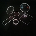
| Model: | 6 inches, 8 in |
|---|---|
| Brand: | - |
| Origin: | Made In Afghanistan |
| Category: | Industrial Supplies / Glass & Ceramics Machine |
| Label: | Wafer cover plate , borofloat 33 wafer , Wafer substrate |
| Price: |
¥100
/ pc
|
| Min. Order: | 1 pc |
| Last Online:07 Jul, 2025 |
learn more custom glass wafer
Precision-Cut Glass Substrates in Borosilicate, Quartz, Fused Silica, and More
Engineered Glass Wafer Solutions Tailored to Your Process Needs
At Lighting, we specialize in the custom fabrication of glass wafers across a wide range of materials, diameters, and surface finishes. Whether you're working on advanced semiconductor packaging, optical MEMS, photonic integration, or biomedical devices, our wafers are optimized for dimensional accuracy, thermal stability, and chemical compatibility with demanding process environments.
Available Materials for Custom Wafers
| Material | Properties | Applications |
|---|---|---|
| Borosilicate Glass (e.g., BOROFLOAT® 33, D263T) | Low thermal expansion, good chemical resistance | Microfluidics, bonding substrates, photolithography |
| Quartz / Fused Silica | High purity, UV/IR transparency, thermal shock resistance | Optoelectronics, UV lithography, vacuum windows |
| Aluminosilicate Glass | High mechanical strength, scratch resistance | Flexible wafers, displays, protective covers |
| Soda Lime Glass | Cost-effective, basic thermal/optical performance | Display testing, general-purpose wafers |
| AF32 / EAGLE XG® / Willow Glass | Ultra-thin, alkali-free, display-grade | Thin semiconductor packaging, flexible electronics |
Custom Wafer Specifications
Diameter Options:
Standard: 2", 3", 4", 6", 8"
Custom: From 10 mm to 300 mm (larger sizes upon request)
Thickness Range:
From 0.1 mm ultra-thin to 5 mm thick for high-pressure or optical systems
Surface Quality:
Ground, single-side polished (SSP), or double-side polished (DSP)
Surface roughness: down to <1 nm RMS
Flatness: λ/10, TTV < 5 µm available for high-precision needs
Edge Options:
Flat, notch, beveled, or laser-cut edge geometries
SEMI standard edge finish or application-specific treatment
Optional Add-ons:
AR / ITO / dielectric coatings
Alignment marks, photomask pre-patterning
Thermal cleaning or vacuum packaging
Industry Applications
Semiconductor Processing – Carrier wafers, RDL/interposer platforms, wafer-level packaging
Microfluidics & BioMEMS – Channel substrates, bonding cover glass, transparent lab-on-chip bases
Optoelectronics – Waveguide substrates, LED test wafers, laser cavity spacers
Photovoltaics – Conductive coatings on glass wafers for solar device prototyping
Optical Measurement & Testing – Metrology-grade substrates, reference flats, calibration plates
Why Choose us for Custom Glass Wafers?
Precision CNC, laser and ultrasonic cutting for clean, crack-free edges
Strict flatness, TTV and parallelism control for wafer bonding and lithography
Compatible with wafer-level automation: vacuum chucks, pick-and-place, UV bonding
Small batch prototyping to mass production support
Fast lead time, engineering drawings review, and technical consultation available
From flexible ultra-thin wafers to optically polished thick substrates, we deliver glass wafer solutions tailored to your fabrication process and end-use performance needs.
learn more custom glass wafer
| Payment Terms: | 0 |
|---|---|


